Test Index
CBSE Class 12 Physics 2023 Outside Delhi Set 3 Paper
© examsnet.com
Question : 9 of 13
Marks:
+1,
-0
With the help of a circuit diagram, explain how a full wave rectifier gives output rectified voltage corresponding to both halves of the input ac voltage.
Solution: 👈: Video Solution
The circuit diagram of a full wave rectifies: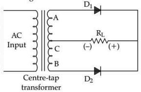 A centre tap transformer and two identical divides and are used to diagram a full wave rectifies. The centre-tap transformer has 3 output terminals. Centre tap is is always at .Drawing positive half cycle of is +ve and is . For negative half cycle, B is + ve and A is - ve. So, when positive half cycle appears, A is +ve, B is and is .So, divide is forward biased and divide is reverse biased.When negative half cycle appears, is -ve, is + Ve and is So, divide is forward biased and divide is reverse biased.So, for each half cycle one divide conducts current through flows unidirectionally. Hence the voltage developed across is a DC.
© examsnet.com
Go to Question: